CCD Camera Information Primer
This is a compilation of information gathered regarding the use of CCD (Charged Coupled Device) camera sensors in laser research. The background information in the subject is pretty sparse. Since the technology has reached maturity just in past few years. No papers were found regarding this topic. And this lack of background suggests that the topic hasn't been explored fully. These report is just a small part of my ongoing project in laser optics. CCD sensors appear to be a fast way to get fast information from laser phenomena. However, there is not much information regarding how accurate this information is. This is the reason that sparked my interest in the subject and why I plan to developed a CCD camera to use in my projects that use laser light. The Charged Coupled Device, or CCD, was co-invented in 1970 by Boyle and Smith at Bell Labs. The CCD chips are one of the wonders of modern solid state technology. They are composed of an array of photosensor baked on a light-sensitive crystalline silicon ship. These photosensitive elements transform incoming light (photons) into voltages that can be stored digitally into discrete values. The electric charges that are produced are stored within metal oxide capacitors (MOS) that function as an electric potential well. These charged are shifted from successive potential wells, using changes in voltage, until they reach an external terminal. This is where the final readout process happens. There are three different types of architecture employed in the manufacturing of CCD cameras. The main difference from all these designs is in how they received and process the information. These designs are:
- Full-Frame CCD
- Interline Transfer CCD
- Frame-Transfer CCD
The Full-Frame CCD
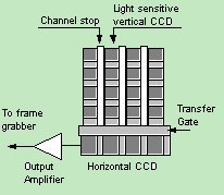
After the exposure the Full-Frame CCD must be covered from
light during the readout process. The charge from the bottom row of
the potential wells is 'shifted' to one side in order to be read one
by one. When the whole row is read, the next row drops down and the
whole process begins again. Once this has been done, the device is
ready to receive the input from another picture.
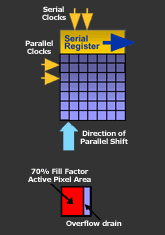
The Inter-line-Transfer CCD
Every second column within an Inter-line-Transfer CCD is covered by an
opaque mask. These covered areas contain the wells that are used in
the readout process. After the exposure, the charged packets in each
exposed cell is shifted into the adjacent opaque masked wells. From
here, the charge is being 'shifted' as in the Full-Frame CCD. The
advantage of this is that while the charge is being 'shifted' the
exposed wells can accumulate in the next image. But, the disadvantage
is that only 50% of the surface is exposed. This method is fairly
rapid.
Frame Transfer CCD
The frame transfer CCD imager has a parallel register divided into two
distinct areas. The upper area is the image array, where images are
focused and integrated. The other area, the storage array, is
identical in size and is covered with an opaque mask to provide
temporary storage for collected charge. After the image array is
exposed to light, the entire image is rapidly shifted to the storage
array. While the masked storage array is read, the image array
integrates charge for the next image. A frame transfer CCD imager can
operate continuously without a shutter at a high rate. The front
illuminated Frame Transfer CCDs suffer the same fate as the Full Frame
CCDs, that is a reduced QE in the visible with a particularly low QE
in the blue. The combination of back illuminated (CCD EEV 57) , the
shutterless operation, relatively high frame rates and very high QE is
very desirable to have in a camera system.
Characteristics
There are many important characteristics that should taken into account when buying a camera. Even when a camera should excel in all categories, the buyer sometimes have to make a compromise. The reason for this is that sometimes some of these features are more expensive to include than other. The following table should will inform about some of the most important features of a CCD camera.
Sensitivity
This defines the electronic variation for a given brightness, the information is usually acquired by comparing the level of brightness on the target to the saturation.
A - Sensitivity
This analyze the variation between different levels of brightness. A higher sensitivity could could be able to detect the minute differences between different levels of brightness.
C - Transfer Function
Transfer Functions analyze the ratio of output modulation to input modulation. This is a mathematical expression that tells you how accurate is the link between the camera output and the light intensity.
D - Resolution
The resolution is determined by the number of sensor elements on the CCD chip. A higher number of elements will increase the detail observed from a particular image. On a CCD camera the resolution is usually defined in the number of pixels for the x and y dimension of the camera. A high resolution will be extremely important when trying to observe the fine details of an image. In order to have high resolution a CCD camera must have:
o At least an array of 1 megapixels. Such as a 1000 by 10000 pixel camera. And must have few bad pixels. Which are pixels that are dead or not responding appropriately.
o A cooling system to reduce thermal noise.
o A high readout clock frequency.
Black and White cameras have an extra edge over Color cameras. Since the resolution for color cameras is reduce by 1/3 compared to a B&W camera of the same pixel count. This is due to the fact that color cameras usually use 3 types of sensor to detect color images, one for Red, one for Blue and another for Green.
F - Low light levels Capture
A camera that has to work with low light level captures must have a low
signal to noise ratio. The least level of light that can be detected must
be higher than the noise level in the system. This sometimes fudges the
low level signals against the background noise. There are many sources for
this noise, such as:
- Fixed Pattern Noise (FPN) which is caused by defects in the sensor
array. This noise pattern is usually constant on all expositions. This
source is usually inversely proportional to the quality of the sensor
array. However higher quality implies a more costly array.
- Thermal noise, which can be reduced by cooling the sensor below 30
- Any uncooled electronic will emit charges which are collected and ad to
the noise level.
- Electronic noise, which is produced by the rapid movement of charges
during the readout process. It can be lowered by choosing moderate clock
frequencies for the charge transfer to the readout section of the system.
- Reset noise, which is produced when not every charge is drained out of
the CCD elements. This charge leftover will influence the value for the
next readout on this CCD element.
G - Capture speed
This is important in any field of optical research since you always want
to have a fast snapshot of viewed system during any event. Since all
events in physics change rapidly with time, a fast camera will reduce the
blurriness of the data observed a system drifting out across time.
The speed of a digital camera depends on several factors:
- The sensor architecture, a full frame digital camera is slower than a frame transfer camera or a interline transfer due to the higher density of the sensor on the chip.
- Number of pixels: the digital cameras, at the same clock frequency, is
fast if it has few pixels.
- Clock frequency, a higher clock frequency makes a fast charge transfer
possible. However, increasing the clock frequency higher than 25 Mhz
increases the signal to noise ratio.
H - Spectral response
This inform us of how efficiently the camera picks up photons of different
wavelength. In laser research this characteristic of the CCD sensor is
highly important since lasers are usually tuned to a very specific
frequency. Usually the detection range of the sensor array is around the
visible range, passing through the infrared and up to 1000 nm. However,
any wavelength other than those, the detection is difficult.
Spectral sensitivity is also referred as Quantum Efficiency (Q.E.). A
perfect CCD sensor has a Q.E of 1. This means that for every photon
falling upon the sensor, an electron or charge is produce. In reality, the
Q.E. Of most cameras max. out at .7. That is, for every 10 photons, 7
electrons are produce by the CCD.
============================================================================
Ways to test a CCD camera performance
There are many ways to test the performance of a CCD camera. All
depends of the criteria that we use to judge the camera. In laser
research, the most important characteristic of the camera, is the
linearity of the incident light versus the charged recorded by the
device. The simplest of the methods would be to just take a picture with
camera covers on. This in theory should produce a totally black image,
devoid of any features or objects. However, most CCD cameras will produce
a dark background with small white spots on it. These are a by product of
thermal noise. Also, the CCD doesn't record the total range of
intensities. The recording is made in discrete zones. With the intensity
value of a small surface elements being the same. The result of this, is
that every small element gives an average value of the light intensity
over that given surface. This leads to another test of the accuracy of the
CCD sensor. A surface composed of a series of dark and bright fringes
could be composed. The camera used to record the image can only show a
finite amount of detail of the lines. If the the number of lines is bigger
than the number of pixels along an axis. A process called aliasing
occurs. Where the frequency of the lines appear to be less than they are
since a section of the fringes had to be sampled as the same value. The
maximum frequency of such changes between intensity that can be recorded
by a camera is called Nyquist frequency.
On the other hand, there are mathematical analysis that can help
us find the quality of the date gathered by our CCD array. One of this
methods is the Modulation Transfer Function (MTF) which measures the ratio
of output modulation versus input modulation and other is the Point Spread
Function (PSF), which measured the how blurred is the image taken compared
with the real object.
Kodak's New Line of CCD camera.
CTE CCD Glossary